Benefits:
- Dramatically improves productivity
- Low cost - Can pay for itself in months
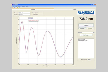
- Accurate - Measure to better than ±1%
- Fast-Measurements in seconds
- Non-Invasive - Totally outside of deposition chamber
- Easy to use - Intuitive Windows® software
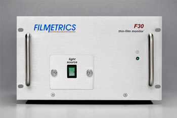
- Turn-key system sets up in minutes
Model Specifications
| Model | Thickness Range* | Wavelength Range |
|---|---|---|
| F30 | 15nm-70µm | 380-1050nm |
| F30-EXR | 15nm - 250µm | 380-1700nm |
| F30-NIR | 100nm - 250µm | 950-1700nm |
| F30-UV | 3nm-40µm | 190-1100nm |
| F30-UVX | 3nm - 250µm | 190-1700nm |
| F30-XT | 0.2µm - 450µm | 1440-1690nm |


